Profile
 Settings
 Refer your friends
 Sign out


A transistor is a linear semiconductor instrument that utilizes a lower-power electrical signal to control current. Bipolar and field-effect transistors are the two major types of transistors. We looked at bipolar transistors in the previous chapter, which use a small current to control a high current. In this chapter, we’ll cover the broad notion of a field-effect transistor—a device that manages current with a modest voltage—before focusing on one specific type: the junction field-effect transistor. We’ll study another form of field-effect transistor, the insulated gate variety, in the next chapter.
Junction Field Effect Transistor
In electronic circuits, the junction field effect transistor, or JFET, is frequently used. The junction field effect transistor is a dependable and useful electronic component that may be utilised in a wide range of electronic circuits, from amplifiers to switch circuits, with great ease.
The junction field effect transistor is a simple semiconductor device that may be purchased for a cheap cost. This makes them perfect for use in a variety of electrical circuits where a strong cost-performance ratio is desired.
JFETs have been around for a long time, and while they don’t have the same high levels of DC input resistance as MOSFETs, they are still quite reliable, robust, and simple to use. As an outcome, these electronic components are a great replacement for a wide range of electronic circuit designs. Also accessible are components in both leaded and surface mount device configurations.

Typical JFET semiconductor device
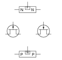
N-channel JFET

The directed current in a junction field-effect transistor, or JFET, flows from source to drain or drain to source, depending on the situation. Between the gate and the source, the regulating voltage is applied. It’s worth noting that the current does not have to pass through a PN junction on its journey from source to drain: the path (known as a channel) is a continuous block of semiconductor material. This channel is an N-type semiconductor in the figure above. JFETs with P-type channels are also obtainable:
P-channel JFET

N-channel JFETs are used more frequently than P-channel JFETs. The reasons for this have to do with nitty-gritty aspects of semiconductor theory that I’d rather not go through in this chapter. I feel that, like bipolar transistors, the best method to introduce field-effect transistors is to ignore theory as much as possible and instead focus on practical characteristics. The biassing of the PN junction created between the gate material and the channel is the only practical distinction between N- and P-channel JFETs you need to think about anymore now.
The channel is a wide-open path for current to pass when no voltage is applied between the gate and the source. However, if a voltage of such polarity is placed between gate and source that reverse-biases the PN junction, the flow between source and drain connections is limited or regulated, just as it was for bipolar transistors with a fixed base current. All current across the source and drain is “pinched off” by the maximum gate-source voltage, forcing the JFET into cut status.
JFET Basics
A field effect transistor, often referred as a FET, is a silicon section whose conductance is regulated by an electric field. The channel is a piece of silicon through which current flows, and it is made up of one of two categories of silicon: N-type or P-type.
The source and drain connections are located on either end of the device. The current is controlled by an electric field provided to a third electrode known as a gate.
The device is considered to be voltage operated since solely the electric field controls the current flowing in the channel. It also has a large input impedance, usually many megohms. This can be a major benefit over a current-operated bipolar transistor with a significantly lower input impedance.
JFET operation
Junction FETs are voltage-controlled transistors. In other terms, voltages applied to the gate control the device’s operation.
Both N-channel and P-channel devices work in the same fashion, with the exception that the charge carriers are inverted in one, resulting in electrons in one and holes in the other. The case for an N-channel device will be discussed as it is the most prevalent.
The thickness of this layer is proportional to the degree of the junction’s reverse bias. In other words, when the reverse bias is small, the depletion layer only extends a little distance into the channel, leaving a vast region for water to pass.
When the gate is subjected to a significant negative bias, the depletion layer expands, reaching further into the channel and minimizing the area over which current can flow.
JFET circuit applications
JFETs are extremely useful electronic components, and they’re used in a number of technological circuit designs. They have a number of distinct benefits that can be used in a multitude of circuits.
Simple biasing
High input impedance
Low noise
JFETs are used in a wide range of circuits, from amplifiers to oscillators, logic switches to filters, and many other applications, due to their characteristics.
JFET structure & fabrication
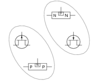
JFETs are available across both N-channel and P-channel configurations. They are fairly identical to one other, with the difference that the N and P areas in the structure below are transposed.
The fabrication of FETs can be done in a variety of ways. A severely doped substrate serves as a second gate in silicon devices.
The active n-type area can then be generated by epitaxy, diffusing impurities into the substrate, or ion implantation. When gallium arsenide is employed, a semi-insulating intrinsic layer is used as the substrate. This minimizes the levels of any stray capacitances, allowing for good high-frequency performance.
JFET characteristics
The various types of JFET characteristics.
1. JFET Drain Characteristic with Shorted-Gate: A junction field effect transistor’s output characteristic can be described in two ways. The first one is when the gate is shorted to 0 volts. This results in a single curve for the semiconductor device, demonstrating how it performs under these conditions.
2. JFET Drain Characteristics with External Bias: It’s also crucial to know how the junction FET behaves when exposed to various amounts of bias. After that, curves representing the attributes under various bias levels are provided.
3. JFET Transfer Characteristic: A junction field effect transistor’s transfer act shows how variations in gate voltage, VGSM, affect the output or drain current, ID.
Conclusion
JFET stands for junction field effect transistor and is a voltage managed current source with extremely high input impedance. Unlike BJT, JFET is a unipolar junction transistor that is utilised as an amplifier in many electronic systems.