P-type and n-type materials were sandwiched with an Intrinsic layer in between the p and n-type materials to create a pin diode. A thermionic valve is a diode with two electrodes (an anode and a cathode which are the p and n-type materials). The core layer functions as an insulator, preventing electricity from passing through it. High-voltage rectifiers, RF switches, microwave switches, variable attenuators and other applications use the PIN diode. Every diode, in general, acts as a one-way valve for current flow and the Pin diode can be utilized in the same way to stop current flow if a relative rise in voltage or current flow is detected. The pin diode and its applications, as well as the input and output characteristics, will be discussed in this article.
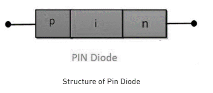
Pin diode is a diode with an undoped intrinsic semiconductor material that is placed in between the p-type semiconductor and an n-type semiconductor region. Compared to the intrinsic area in the junction, the p-type and n-type regions are usually extensively doped. The end terminals of these PIN diodes were employed for ohmic contacts, making them broader than regular p-n diodes.
In contrast to regular p-n junctions, the PIN diode has a larger intrinsic region, making it a unique diode for a variety of applications. Because of the broader intrinsic layer, which provides a constant resistance to current flow, this diode is thought to be a resistor when used in a circuit.
The pin diode’s construction is typically cylindrical, with all three layers sandwiched and the whole diode is covered in plastic hosing, leaving two ohmic contacts for circuit connection. In the structure of the PIN diode, holes are the majority charge carriers in the P-type material, whereas electrons are the predominant charge carriers in the N-type material.
Jun-ichi Nishizawa and his colleagues devised the PIN photodiode in the late 1950s. For some applications, it is a substitute for the PN-junction. The PN-junction diode was first employed as a high-power rectifier with low frequency in electric circuits after its development in the 1940s.It is well known that the presence of an intrinsic layer between the p-n junction raises the breakdown voltage for high-voltage detection. It can also be used for high-voltage applications such as radio and microwaves. Because of the sequence in which the P-type material, Intrinsic layer and N-type material were inserted inside the diode, it was given the moniker PIN diode.
The charge carriers will flow from the N-type region to the intrinsic region when the PIN diode is unbiased due to charge carrier concentration in a certain region. As a result, at the N-I junction, the depletion region becomes wider. As a result, width is greater on the N-side and less on the I-side.
This is due to the fact that N-type material is strongly doped, whereas the Intrinsic layer is not. As a result, a depletion area is created when charge carriers (electrons are the majority carriers on the N-side) flow from the N-type to the Intrinsic layer, but the breadth of the depletion region on either side of the N-P junction will be different.
When compared to other types of diodes, the pin diode has a broader junction. When linked in reverse-biassed mode, the pin diode’s capacitance is reduced due to the larger surface. The depletion region created here is substantially larger and the size of the region remains nearly constant even when the biassing voltage is varied widely.
The charge carriers travel into the depletion region during forward biassing and the current flow begins as the holes and electrons get closer.
During reverse biassing, the intrinsic layer between the P and N layers widens the gap between the two layers, lowering the diode’s capacitance. As a result, the diode is isolated.
Rf (radio frequency) switches, voltage rectifiers, microwave switches, variable attenuators and photodiodes are some of the most common uses.
🡪Pin diodes act as voltage changeable resistors as RF switches and microwave frequency switches and they can provide significantly better levels of consistency than RF relays, which are typically the only other available diodes.
🡪The intrinsic layer in the diode creates a gap between the two layers as a voltage rectifier, allowing the layers to withstand larger reverse voltages. It’s used where a gadget that uses high voltages is used.
🡪All of the principal applications of the diode as a voltage changeable resistor as a variable compensator were based on this property. To make a variable attenuator, three diodes can be used to replace the circuit’s fixed resistors and similar circuits have been developed for circuits.
🡪It turns light into current in the depletion area of a photodiode in the form of a photodiode. When the intrinsic layer is inserted, the depletion zone expands, which improves performance by increasing the volume of light change.
The following are some of the benefits of using a pin diode:
🡪It is necessary to use a very low reverse bias voltage.
🡪Quantum efficiency is high.
🡪It is possible to gain a bigger bandwidth.
🡪Other diodes have lower noise performance, higher efficiency and are more cost effective.
🡪The larger depletion region gives additional working space.
🡪Large resistance (tolerance) to reversal voltage increases.
The biggest drawback is that it is unable to enhance the signal that passes through it.
🡪Sensitivity is low, and it fluctuates as the temperature changes.
🡪Very intricate packing that, if misplaced without precision, can cause the PIN diode to fail.
🡪When compared to a conventional diode, the recovery period after a power loss is substantially longer.
The only difference between a pin diode and a regular p-n junction diode is the intrinsic layer in the middle of the diode. The depletion zone at the p-n junction shrinks as the PIN diode is subjected to forward bias and current begins to flow through the diode. The area of the depletion region grows when the PIN diode is placed to reverse the biassed state. The depletion layer evaporates entirely at a lower reverse bias voltage. When the pin diode is low biassed, the capacitance of the pin diode decreases and the intrinsic area widens. Because of the intrinsic layer, the PIN diode offers a wide range of applications. Pin diode is a diode with an undoped intrinsic semiconductor material that is placed in between the p-type semiconductor and an n-type semiconductor region.
 Profile
 Settings
 Refer your friends
 Sign out