In this topic, we will learn about the NOT gate operation, the meaning of NOT gate, its geometrical symbol, truth table, boolean expression and implementation of NOT gate and the circuit for NOT gate realisation.
The logic gate is an electronic circuit that follows a certain logical relation between the inputs and outputs. That is, it makes the logical decisions regarding the existence of outputs depending on the nature of inputs.
George Boolean (1815-1864), an English mathematician, had developed certain algebraic operations for dealing with the mathematical analysis of logic. It is called Boolean algebra. The logic mainly contains only two values, either ‘high’ or ‘low’; ‘closed’ or ‘open’; ‘ON’ or ‘OFF’; ‘true’ or ‘false’ etc., by 1 and 0, respectively.
Therefore, only two states or values can be represented through Boolean algebra for any variable. These two values or states represent Boolean algebra containing three operations. They are called: OR, AND, and NOT. These are the relations between inputs denoted by A, B etc., and the output is denoted by Y.
NOT Operation
The operation NOT can be represented by the ganged switch. If switch A is closed, then B is automatically opened and vice-versa.
The operation can be represented in the following table.
The NOT operation, in boolean algebra, is mainly denoted by a bar or dash over the variable. Thus, the Boolean expression is given by
Y = A’
The above boolean expression is verbally expressed as Y is not A. It states that the output Y does not exist when the input A exists and vice versa.
NOT Gate meaning
A digital electronic device in which the output is NOT the same as the input is called NOT gate. So, the NOT gate has only one input, and this input is inverted to only one output. The NOT gate has only two terminals, one which contains input data and the other where the output is generated. The input may be denoted by A and output by Y.
Geometrical Symbol:
In the circuit diagram, the NOT gate is represented as shown in the below figure:
In the above figure, the bubble at the right end of the triangle is called the invert bubble because the NOT gate inverts, compliments, or negates the input.
Boolean expression:
In terms of the Booleans algebra, the operation of NOT gate is denoted as follows:
It implied Y equals NOT A. The bar over the symbol A means NOT.
Truth Table:
A truth table is defined as the table that shows all the relevant combinations of the inputs and their corresponding outputs. In order to create a truth table, we need to use binary digits 1 and 0. A = 1 denotes that input A exists, and Y = 1 suggests that output Y exists. The existence may be designated as 1 or ON, and non-existence may be denoted as 0 or OFF.
NOT gate combination of the input and corresponding output can be depicted in the truth table, which is shown below:
Circuit for NOT Gate realisation
In a transistor amplifier, the input signal is inverted, so due to this reason, in place of a diode, the common-emitter configuration is used in a transistor amplifier. Thus, the phase of the signal is changed due to this configuration.
The digital circuit containing NOT gate is shown below:
Two general cases may happen in the above circuit:
When A = 0: When A is connected to the grounded terminal of the battery, there is no collector current flowing through the emitter-base junction as the junction is reversed biassed. The potential drop across R₁ reduces to zero because the transistor potential is cut off. Therefore, the voltage of the battery at C and the voltage at the output terminal (Y) will be the same or equal, that is +5 V. Hence, Y = 1.
When A = 1: When A is connected to the +5 V terminal of the battery, a large amount of the collector current flows at the emitter-base junction through R₁ as the junction is forward biassed. Therefore, the voltage of the battery at C and the voltage drop across R₁ will be the same as the transistor is in a saturated state. Furthermore, collector C will be grounded through the conducting transistor. Hence, Y = 0.
Conclusion
The NOT gate is a logic gate that can accept only one input and gives out only one output. So, the NOT gate has only one input, and this input is inverted to only one output. It is a primary gate used to create other useful gates such as NAND, NOR, etc. It also creates a square wave oscillator. It can be implemented by using universal gates as well as diodes. The IC number of NOT gate is 7404.
Frequently asked questions
Get answers to the most common queries related to the IIT JEE Examination Preparation.
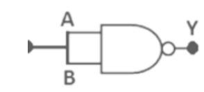
Construct the NOT gate from the NAND gate.
Ans. The NAND gate can be considered the digital electronic building block as all the primary gates like OR,...Read full
Why is a NOT gate known as an inverter circuit?
Ans. A NOT gate gives output for no input and vice-versa. In other words, a NOT gate puts the input conditions in...Read full
What is a saturation state in a NOT gate?
Ans. For maximum collector current, the values of collector circuit resistance and base circuit resistance are ad...Read full
What are added and subtractor circuits?
Ans. The combination of the basis gates that OR gates, AND gate and NOT gate to perform complex mathematical func...Read full
Ans. The NAND gate can be considered the digital electronic building block as all the primary gates like OR, AND, and NOT gates can be constructed through it.
NOT gate can be constructed using NAND gate; when both the NAND gate inputs (A and B) are joined together, it works as the NOT gate. In this case, the NAND gate has only one input and one output which is shown in the figure below:
Ans. A NOT gate gives output for no input and vice-versa. In other words, a NOT gate puts the input conditions in the opposite order; that is, it inverts the input order. Thus, it is known as an inverter circuit
Ans. For maximum collector current, the values of collector circuit resistance and base circuit resistance are adjusted in a NOT gate. This state of the NOT gate is known as the saturation state.
Ans. The combination of the basis gates that OR gates, AND gate and NOT gate to perform complex mathematical functions are known as adder and subtractor.
Crack IIT JEE with Unacademy
Get subscription and access unlimited live and recorded courses from India’s best educators
Get all the important information related to the JEE Exam including the process of application, important calendar dates, eligibility criteria, exam centers etc.
 Profile
 Settings
 Refer your friends
 Sign out