Profile
 Settings
 Refer your friends
 Sign out


A NAND gate can be implemented by cascading an ‘AND’ gate and a ‘NOT’ (N) gate. There can be two or more inputs to a NAND gate; however, there is only one output. It can also be referred to as a negated AND gate.
The expression for a NAND gate can be written as In Boolean algebra, a NAND gate is considered a universal gate since it can be used to implement all basic gates such as AND, OR and NOT. It can also be used to implement the other universal gate, NOR. This property of the NAND gate can also be termed functional completeness.
Truth table
The truth table for a two-input NAND:
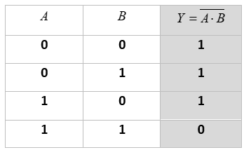
From the truth table, it can be seen the output is true (1) if at least one of the inputs is false (0). When all inputs are true (1), the output is false (0).
The truth table for a three-input NAND gate can be represented as follows:
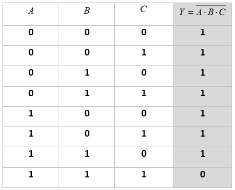
In this table also, it can be seen that the output is always true (1) if at least one of the inputs is false (0). When all inputs are true (1), the output is false (0).
Circuit diagram
A NAND gate can be obtained by cascading an AND gate and a NOT gate as follows:

From the above diagram, we can see that the output of the AND gate is being inverted. Instead of adding a separate NOT gate, we can simply add a bubble at the output of the AND gate. The bubble will indicate an inversion at the output. Therefore, the circuit symbol for a NAND gate is as follows:

According to the first law of De Morgan, From this theorem, we can say that the circuit for
will be equivalent to the circuit for
Therefore, a circuit for
can be illustrated as:

Instead of using a NOT gate, we can use bubbles at the input, indicating an inversion as follows:

Therefore, it can be said that a NAND gate and a bubbled OR gate are equivalent.

Universal gate
A NAND gate can be used to implement a NOT gate, AND gate, OR gate, NOR gate, Ex-OR and Ex-NOR gate.
Implementing NOT gate
To implement a NOT gate using a NAND gate, we tie the inputs of the NAND gate, that is, give two same inputs. The output expression will be:
[Using the law of idempotency
]Implementation of NOT using NAND can be illustrated as follows:

Implementing AND gate
To implement an AND gate, we invert the output of a NAND gate. The output expression will be:
[Using the property of double inversion
Implementation of AND using NAND can be illustrated as follows:

It can be seen that the output of the first NAND gate is inverted to obtain an AND gate. The inversion is done using a NOT gate, which has been implemented using a NAND gate.
Implementing OR gate
To implement an OR gate, we invert the input of a NAND gate. The output expression will be:
[Using the De Morgan law
]
[Using the property of double inversion
Implementation of OR using NAND can be illustrated as follows:

It can be seen that the two inputs to the NAND gate on the right are inverted to obtain an OR gate.
Implementing NOR gate
To implement a NOR gate, we invert the input as well as the output of a NAND gate. The output expression will be:
[Using the De Morgan law
[Using the property of double inversion
Implementation of NOR using NAND can be illustrated as follows:

Implementing Ex-OR gate
Implementation of Ex – OR using NAND can be illustrated as follows:

[Using the De Morgan law
]
[Using the property of double inversion
]
[Using absorption law
]
Similarly,
[Using the De Morgan law
]
[Using the property of double inversion
]
[Using absorption law
]
Finally,
[Substituting value of Y and Z]
[Using the first De Morgan law
]
[Using the second De Morgan law
]
[Using the property of double inversion
]
Implementing Ex-NOR gate
Implementation of Ex – NOR using NAND can be illustrated as follows:

The output expression from the above diagram can be illustrated as follows:
[Using the law of idempotency
]
Similarly,
[Using the law of idempotency
]
Now,
[Substituting the value of Y and Z]
[Using the first De Morgan law
]
[Using the property of double inversion
]
Finally,
[Substituting values of X and P]
[Using the first De Morgan law
]
[Using the property of double inversion
]
[Using the second De Morgan law
Conclusion
A NAND gate is obtained from a combination of ‘NOT’ (N) gate and ‘AND’ gate. The output of a NAND gate can be represented as The output will always be true (1) if at least one of the inputs is false (0). If all inputs are true (1), the output will be false (0).
A NAND gate can be represented using an AND gate with a bubble or an inversion at the output. A NAND gate is a universal gate, that is, it can be used to implement other basic gates as well as NOR, XOR and EXOR gates.