Access free live classes and tests on the app
Download
+
Unacademy
  • Goals
    • AFCAT
    • AP EAMCET
    • Bank Exam
    • BPSC
    • CA Foundation
    • CAPF
    • CAT
    • CBSE Class 11
    • CBSE Class 12
    • CDS
    • CLAT
    • CSIR UGC
    • GATE
    • IIT JAM
    • JEE
    • Karnataka CET
    • Karnataka PSC
    • Kerala PSC
    • MHT CET
    • MPPSC
    • NDA
    • NEET PG
    • NEET UG
    • NTA UGC
    • Railway Exam
    • SSC
    • TS EAMCET
    • UPSC
    • WBPSC
    • CFA
Login Join for Free
avtar
  • ProfileProfile
  • Settings Settings
  • Refer your friendsRefer your friends
  • Sign outSign out
  • Terms & conditions
  • •
  • Privacy policy
  • About
  • •
  • Careers
  • •
  • Blog

© 2023 Sorting Hat Technologies Pvt Ltd

Watch Free Classes
    • Free courses
    • JEE Main 2024
    • JEE Main 2024 Live Paper Discussion
    • JEE Main Rank Predictor 2024
    • JEE Main College Predictor 2024
    • Stream Predictor
    • JEE Main 2024 Free Mock Test
    • Study Materials
    • Notifications
    • JEE Advanced Syllabus
    • JEE Books
    • JEE Main Question Paper
    • JEE Coaching
    • Downloads
    • JEE Notes & Lectures
    • JEE Daily Videos
    • Difference Between
    • Full Forms
    • Important Formulas
    • Exam Tips
JEE Exam » JEE Study Material » Physics » AND Gate

AND Gate

In this topic, we will learn the meaning of AND gate, the circuit symbol, truth table, boolean expression, and implementation of AND gate.

Table of Content
  •  

Introduction to AND Gate – AND gate is a type of logic gate where a logic gate is an electronic circuit that follows certain logical relations between the inputs and the outputs. It is a basic digital gate. The inputs and output only contain two values: ‘ 1’ or ‘0’, ‘high’ or ‘low’, ‘true’ or ‘false’, ‘closed’ or ‘open’, ON’ or ‘OFF’ etc. 

Meaning of AND Gate – AND gate is a digital electronic logical gate that takes input and performs multiplication on them. The output is the product of inputs. If all the inputs are set to high or ‘1’, only then the AND gate will give a high output, that is ‘1’.

The Circuit Symbol of AND Gate

The circuit symbol of an AND gate is a ‘D’ shape with input lines on the left side and one output line on the right side of the ‘D’. The circuit diagram of an AND gate with two inputs is given as  

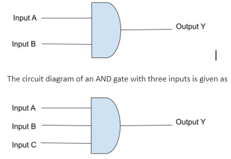
The circuit diagram of an AND gate with three inputs is given as 

Boolean Expression of AND Gate

In Boolean Algebra, a single dot(.) is used to represent AND function.

The boolean expression for a two-input AND is given as

Y=A.B 

The above expression is read as Y is equal to A AND B where A and B are the inputs and Y is the output.

Similarly, the boolean expression for a three-input AND function is given as
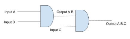
Y=A.B.C 

The above expression is read as Y is equal to A AND B AND C where A, B and C are the inputs and Y is the output.

Truth Table of AND Gate

A truth table is a table that shows all the combinations of input and their corresponding outputs. Binary digits are used in the truth table. The AND logic is that the output Y will be true only when all the inputs are set high, which means all the inputs should have a value of 1.

The truth table of a two-input AND gate is given as

A

B

Y

0

0

0

0

1

0

1

0

0

1

1

1

In the above table, there are four combinations of two inputs. The output is false for the first three inputs as the product of ‘0 AND 0’, ‘0 AND 1’, or ‘1 AND 0’ is always zero. Only the last combination of the inputs ‘1 AND 1’ gives a true output as it satisfies the AND logic.

The truth table of AND gate with three inputs A, B, C, and one output Y  is given as

A

B

C

Y

0

0

0

0

0

0

1

0

0

1

0

0

0

1

1

0

1

0

0

0

1

0

1

0

1

1

0

0

1

1

1

1

In the above table, there are eight combinations of three inputs. The output is false for the first seven combinations as their product is always zero. Only the last combination of the inputs ‘1 AND 1 AND 1’ gives a true output as it satisfies the AND logic.

Implementation of AND Gate

The logic gates can be implemented using diodes and universal logic gate NAND.

  • Using Diodes

A Diode is an electronic component. It allows the flow of current in one direction only. AND gate can be implemented by using two diodes and a resistor.

When both the inputs A and B are high, both the diodes are reverse biased, and no current is passed to the ground. There is no voltage drop across the resistor. Hence, the output, in this case, is ‘high’.

When both the inputs are low, the current flows through the diodes and the resistor and gives a ‘low’ output. When one of the inputs is low and the other is high, then one of the diodes becomes forward biased and the other reverse biased and gives a ‘low’ output.

  • Using Universal gate NAND

Logic AND can be implemented by using two NAND gates. To implement AND logic, give inputs A and B to gate 1 and then redirect the output of gate 1 to both the inputs of gate 2. The output of the NAND gate 2 will be the same as the output of an AND logic.

Conclusion

The AND gate is a logic gate that can accept two or more inputs but gives out only one output. It can be implemented by using universal gates as well as diodes. In digital electronics, data transmissions and alarm circuits are monitored by using AND gates. Digital measuring instruments also use AND gates. The IC number of AND gates are  7408 and 7411.

faq

Frequently asked questions

Get answers to the most common queries related to the JEE Examination Preparation.

Are AND gate and NAND gate the same?

Ans : No, AND and NAND are not the same. AND gives output as the product of the inputs, while NAND gives output as t...Read full

What is the IC number of the two-input AND gate?

Ans : IC 7408 is a two-input AND gate. There are 14 pins. Pin 7 and pin 14 are used for grounding and power supply. ...Read full

What is the IC number of the three-input AND gate?

Ans : IC 7411 is a three-input AND gate. It consists of three AND gates. Either of the gates can be used irrespectiv...Read full

How can we implement an AND logic consisting of three inputs by using IC 7408?

Ans : IC 7408 takes only two inputs. To implement a three-input AND relation using IC 7408, take two gates, say G...Read full

Ans : No, AND and NAND are not the same. AND gives output as the product of the inputs, while NAND gives output as the negated product of the inputs. In simple words, NAND is the negation of AND. For example, if we consider a gate of two inputs, the output from the AND gate will be ‘high’ only when both the inputs are ‘high’, but in the case of the NAND gate, the output will be ‘low’ only when both the inputs will be ‘high’.


Ans : IC 7408 is a two-input AND gate. There are 14 pins. Pin 7 and pin 14 are used for grounding and power supply. It consists of four AND gates. Either gate can be used irrespective of their order of position. Pins (1, 2, 3), (4, 5, 6), (10, 9, 8) and (13, 12, 11) make four AND  and 3, 6, 8, 11 are the respective output pins.

Ans : IC 7411 is a three-input AND gate. It consists of three AND gates. Either of the gates can be used irrespective of their order of position. Pins (1, 2, 13, 12), (3, 4, 5, 6), and (11, 10, 9, 8) make three AND gates, and 12, 6, 8 are the respective output pins.

Ans : IC 7408 takes only two inputs. To implement a three-input AND relation using IC 7408, take two gates, say G1 and G2, give A and B as the inputs of G1, and redirect the output of G1 as one of the inputs of G2. Give C as the second input of G2. The output of G2 is the output of the three inputs A, B and C.


Crack IIT JEE with Unacademy

Get subscription and access unlimited live and recorded courses from India’s best educators

  • Structured syllabus
  • Daily live classes
  • Ask doubts
  • Tests & practice
Learn more

Notifications

Get all the important information related to the JEE Exam including the process of application, important calendar dates, eligibility criteria, exam centers etc.

Allotment of Examination Centre
JEE Advanced Eligibility Criteria
JEE Advanced Exam Dates
JEE Advanced Exam Pattern 2023
JEE Advanced Syllabus
JEE Application Fee
JEE Application Process
JEE Eligibility Criteria 2023
JEE Exam Language and Centres
JEE Exam Pattern – Check JEE Paper Pattern 2024
JEE Examination Scheme
JEE Main 2024 Admit Card (OUT) – Steps to Download Session 1 Hall Ticket
JEE Main Application Form
JEE Main Eligibility Criteria 2024
JEE Main Exam Dates
JEE Main Exam Pattern
JEE Main Highlights
JEE Main Paper Analysis
JEE Main Question Paper with Solutions and Answer Keys
JEE Main Result 2022 (Out)
JEE Main Revised Dates
JEE Marking Scheme
JEE Preparation Books 2024 – JEE Best Books (Mains and Advanced)
Online Applications for JEE (Main)-2022 Session 2
Reserved Seats
See all

Related articles

Learn more topics related to Physics
Zinc-Carbon Cell

The battery you use every day in your TV remote or torch is made up of cells and is also known as a zinc-carbon cell. Read on to know more.

ZEROTH LAW OF THERMODYNAMICS

Read about the Zeroth law of thermodynamics. Learn about the zeroth law definitions and their examples.

Zener Diode As A Voltage Regulator

Understand the concepts of Zener diodes. Also, learn about the efficiency and limitations of Zener Diode as a Voltage Regulator.

Zener diode as a voltage regulator

zener diode is a very versatile semiconductor that is used for a variety of industrial processes and allows the flow of current in both directions.It can be used as a voltage regulator.

See all
Access more than

10,505+ courses for IIT JEE

Get subscription

Trending Topics

  • JEE Main 2024
  • JEE Main Rank Predictor 2024
  • JEE Main Mock Test 2024
  • JEE Main 2024 Admit Card
  • JEE Advanced Syllabus
  • JEE Preparation Books
  • JEE Notes
  • JEE Advanced Toppers
  • JEE Advanced 2022 Question Paper
  • JEE Advanced 2022 Answer Key
  • JEE Main Question Paper
  • JEE Main Answer key 2022
  • JEE Main Paper Analysis 2022
  • JEE Main Result
  • JEE Exam Pattern
  • JEE Main Eligibility
  • JEE College predictor
combat_iitjee

Related links

  • JEE Study Materials
  • CNG Full Form
  • Dimensional Formula of Pressure
  • Reimer Tiemann Reaction
  • Vector Triple Product
  • Swarts Reaction
  • Focal length of Convex Lens
  • Root mean square velocities
  • Fehling’s solution
testseries_iitjee
Subscribe Now
. document.querySelector('.targetTopBtn').onClick = topFunction; function topFunction() { window.scrollTo({ top: 0, behavior: 'smooth' }) }
Company Logo

Unacademy is India’s largest online learning platform. Download our apps to start learning


Starting your preparation?

Call us and we will answer all your questions about learning on Unacademy

Call +91 8585858585

Company
About usShikshodayaCareers
we're hiring
BlogsPrivacy PolicyTerms and Conditions
Help & support
User GuidelinesSite MapRefund PolicyTakedown PolicyGrievance Redressal
Products
Learner appLearner appEducator appEducator appParent appParent app
Popular goals
IIT JEEUPSCSSCCSIR UGC NETNEET UG
Trending exams
GATECATCANTA UGC NETBank Exams
Study material
UPSC Study MaterialNEET UG Study MaterialCA Foundation Study MaterialJEE Study MaterialSSC Study Material

© 2025 Sorting Hat Technologies Pvt Ltd

Unacademy
  • Goals
    • AFCAT
    • AP EAMCET
    • Bank Exam
    • BPSC
    • CA Foundation
    • CAPF
    • CAT
    • CBSE Class 11
    • CBSE Class 12
    • CDS
    • CLAT
    • CSIR UGC
    • GATE
    • IIT JAM
    • JEE
    • Karnataka CET
    • Karnataka PSC
    • Kerala PSC
    • MHT CET
    • MPPSC
    • NDA
    • NEET PG
    • NEET UG
    • NTA UGC
    • Railway Exam
    • SSC
    • TS EAMCET
    • UPSC
    • WBPSC
    • CFA

Share via

COPY