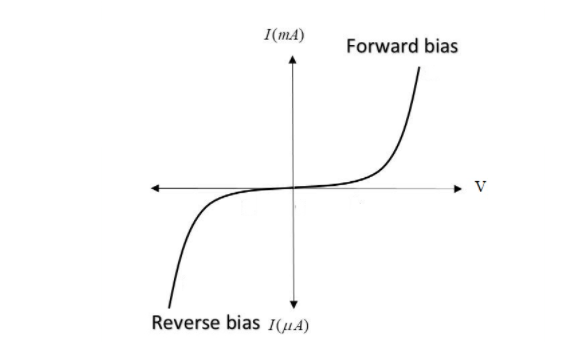
The relationship between the current flowing through the diode and the voltage due to the applied voltage in forward bias and reverse bias is shown by a graph. Thus showing the voltage and diode current through the graph is called VI characteristics of the diode.
If = forward bias current
Vf = forward bias voltage
VR= reverse bias voltage
The PN junction diode is made by combining p and n-type semiconductors with a blocking force between the two semiconductors. The forward current value depends on the amount of forward voltage having a direct relationship between the two. This relation is called IV Characteristics of PN Junction.
In a p-n junction diode, there are two active regions:
P-type
N-type
The voltage applied determines one of three biassing conditions for p-n junction diodes:
A curve between the voltage and current through the circuit defines the V-I properties of P-N junction diodes. The x-axis represents voltage, while the y-axis represents current. Suppose the V-I characteristics of the p-n junction diode are plotted on a graph; we can see that the diode works in three different zones, which are:
No external voltage is delivered to the p-n junction in a zero bias condition,
As a result, the potential barrier at the junction prevents current flow.
As a result, when V = 0, the circuit current is zero.
The p-type of the p-n junction forward bias is connected to the positive terminal of the external voltage, while the n-type is connected to the negative terminal.
As a result, the potential barrier is minimised.
The forward V-I characteristic of the P-N junction diode shows that the current grows exceptionally slowly at the beginning. The curve is nonlinear because the external voltage delivered to the p-n junction is used to overcome the potential barrier in this region.
The potential barrier is removed once the external voltage surpasses the possible barrier voltage and the p-n junction functions like an ordinary conductor. As a result, the curve AB climbs significantly as the external voltage rises, which is nearly linear.
The p-type of the p-n junction is attached to the negative terminal of the external voltage, while the n-type is connected to the positive terminal.
As a result, the potential barrier at the intersection is enhanced.
The junction resistance rises to an extremely high level and virtually no current flows through the circuit.
In practice, however, a very modest current of the order of micro-amperes travels across the circuit. Because of the minority carriers in the junction, this is known as reverse saturation current.
When battery voltage is applied on the forward bias junction, a constant current will flow via this junction.
IS is the saturation current flow (10-9 to 10-18 A)
VT is the volt-equivalent temperature ( 26 mV at room temperature)
n is the emission collision
In fact, this expression is accurate.
When a pn junction is conjoint in a battery in that its n-type region is connected to the positive power of the battery and p-type region is connected to the negative power of the battery, then the pn junction is said to be in reverse biassed condition. Ideally, no current flows through the junction. But in reality, there will be a small reverse bias current which is expressed as iD.
iD drops down to a zero value or least value. iD can be written as i0.
IS is the saturation current flow (10-9 to 10-18 A)
VT is the volt-equivalent temperature ( 26 mV at room temperature)
n is the emission colligation
In fact, this expression is approximate.
The diode’s capacity to work as two separate but equally effective devices makes it a very versatile component. The different types of biassing effects provide you with complete choice over which function the diode will perform in your circuit design. The use of forward bias and reverse bias gives the circuit designer complete control of the diode operation.
Study material notes on 1- V characteristics in forward bias and reverse bias, we can get at a fact – a PN junction diode conducts current only in one direction – i.e. during forward bias. During forward bias, the diode conducts current with an increase in voltage. During reverse bias, the diode does not conduct with an increase in voltage.
 Profile
 Settings
 Refer your friends
 Sign out