Access free live classes and tests on the app
Download
+
Unacademy
  • Goals
    • AFCAT
    • AP EAMCET
    • Bank Exam
    • BPSC
    • CA Foundation
    • CAPF
    • CAT
    • CBSE Class 11
    • CBSE Class 12
    • CDS
    • CLAT
    • CSIR UGC
    • GATE
    • IIT JAM
    • JEE
    • Karnataka CET
    • Karnataka PSC
    • Kerala PSC
    • MHT CET
    • MPPSC
    • NDA
    • NEET PG
    • NEET UG
    • NTA UGC
    • Railway Exam
    • SSC
    • TS EAMCET
    • UPSC
    • WBPSC
    • CFA
Login Join for Free
avtar
  • ProfileProfile
  • Settings Settings
  • Refer your friendsRefer your friends
  • Sign outSign out
  • Terms & conditions
  • •
  • Privacy policy
  • About
  • •
  • Careers
  • •
  • Blog

© 2023 Sorting Hat Technologies Pvt Ltd

Watch Free Classes
  • NEET 2024
  • NEET Answer Key 2024
  • NEET 2024 Preparation Toolkit
  • NEET Rank Predictor 2024
  • NEET College Predictor 2024
  • Study Materials
  • Notifications
  • NEET Syllabus 2024
  • NEET Question Paper
  • NEET Notes
  • NEET Books
  • NEET Paper Pattern
  • Video Lectures
  • Mind Maps
  • Downloads
  • Difference Between
  • Full Forms
  • Exam Tips
  • MCQs
NEET UG 2026 » NEET UG Study Material » Physics » P-n Junction
neetug_toolkit

P-n Junction

In this article, we will study about p-n junction, its properties, basing, p-n junction formula, V-I characteristic of p-n junction diode, manufacture, applications and more.

Table of Content
  •  

Introduction 

What is a p-n junction?

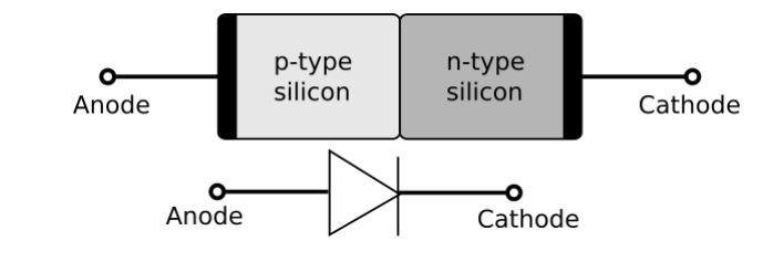
A p–n junction is a boundary or interface between two types of semiconductor materials, p-type and n-type, within a single crystal of semiconductor. In the outer shells of the electrically neutral atoms on the “p” (positive) side there are more holes than electrons on the “p” (+ve) side, while there are more electrons on the “n” (negative) side. This allows only one direction of electrical current to travel through the junction. Doping, such as ion implantation, diffusion of dopants, or epitaxy, creates the p-n junction (growing a layer of crystal doped with one type of dopant on top of a layer of crystal doped with another type of dopant )..

Properties

For modern electronics, the p–n junction has critical features. The conductivity of a p-doped semiconductor is comparatively high. The same is true of an n-doped semiconductor, but depending on the relative voltages of the two semiconductor zones, the junction between them can become depleted of charge carriers and hence non conductive. P–n junctions are often used as diodes, circuit devices that allow electricity to flow in one direction but not the other (opposite) direction, by managing this non-conductive layer. Bias is the application of a voltage across a p–n junction, with forward bias allowing for easy current flow and reverse bias allowing for little or no current flow.

Biasing

Equilibrium (zero bias)

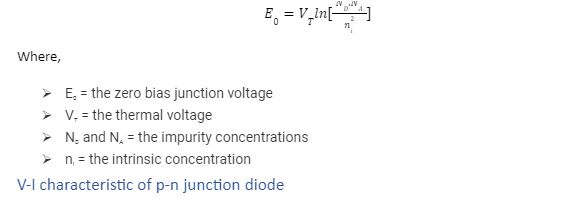
Without an external applied voltage, a p–n junction reaches an equilibrium situation in which a potential difference arises across the junction. Built-in potential(Vbi) is the term for this potential difference.

The free electrons in the n-type are attracted to the positive holes in the p-type at the junction. They disperse into the p-type, where they join with the holes to cancel each other out. The positive holes in the p-type are attracted to the free electrons in the n-type in a similar way. The holes diffuse into the n-type, where they mix with the free electrons and cancel out. In the n-type, the positively charged donor dopant atoms are fixed in the crystal and cannot migrate. As a result, a region near the junction becomes positively charged in the n-type. The p-negatively type’s charged acceptor dopant atoms are fixed in the crystal and cannot migrate. As a result, a region near the junction in the p-type becomes negatively charged. As a result of the electric field created by these charged regions, a region near the junction acts to repel mobile charges away from the junction. The space charge zone, also known as the depletion layer, is formed when regions near the p–n interface lose their neutrality and most of their mobile carriers.

Forward bias of the p-n junction

When the p-type is linked to the positive terminal and the n-type to the negative terminal of the battery, the p-n junction is said to be forward-biased. The built in electric field at the p-n junction and the applied electric field are in opposite directions when the p-n junction is forward biased. When both electric fields are combined together, the resultant electric field is smaller than the built-in electric field. As a result, the depletion region becomes thinner and less resistive. When the applied voltage is high, the resistance of the depletion area becomes insignificant. At 0.6 V, the resistance of the depletion zone in silicon becomes entirely negligible, allowing current to flow freely over it.

Reverse bias of the p-n junction

The p-n junction is said to be reverse biased when the p-type is linked to the negative terminal and the n-type is attached to the positive side of the battery. In this circumstance, the applied electric field and the built-in electric field are both pointing in the same direction. The resultant electric field is in the same direction as the built-in electric field, resulting in a more resistive, thicker depletion area. The depletion region gets more resistance and thicker when the applied voltage is increased.

p-n junction formula

The p-n junction formula, which is based on the built-in potential difference induced by the electric field, is as follows:

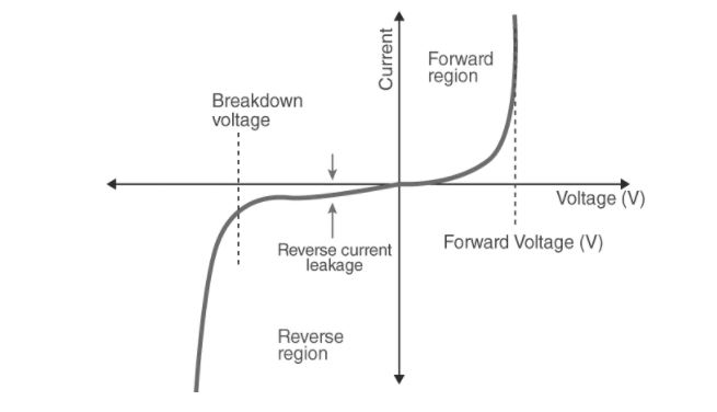
A curve between the voltage and current through the circuit defines the VI properties of PN junction diodes. The VI characteristics curve of the PN junction diode is shown in the graph above. In this curve, we can see that the diode works in three different zones, which are:

  • Zero bias 
  • Forward bias
  • Reverse bias

There is no external voltage delivered to the PN junction diode when it is at zero bias, which implies the potential barrier at the junction prevents current passage.

Applications of p-n junction diode

  • When the p-n junction diode’s arrangement is reverse-biased, the diode can be used as a photodiode because it is sensitive to light.
  • It has the potential to be used as a solar cell.
  • The diode can be employed in LED lighting applications when it is forward-biased.
  • Many electric circuits use it as a rectifier.

Conclusion

  • The p-n junction is the fundamental component of all s/c devices. Understanding junction theory is essential for comprehending other s/c devices.
  • Uncompensated -ve ions (N,’) on the p-side and uncompensated +ve ions (Np*) on the n-side create a p-n junction. As a result, a depletion region formed near the intersection.
  • Drift current (due to the electric field) is balanced by diffusion current (due to concentration gradients of the mobile carriers) at thermal equilibrium.
  • When +V is supplied to the p-side, a substantial current flows across the junction, however when —-V is applied, no current flows at all.
faq

Frequently asked questions

Get answers to the most common queries related to the NEET UG Examination Preparation.

In a PN junction diode, how does current flow?

Ans: When the voltage is increased, electrons move from the n-side to the p-side of the junction. The movement of ho...Read full

What causes reverse saturation current and why does it exist?

Ans: From 0 volts to break down voltage, the reverse saturation current is the negligibly small current (in the rang...Read full

What happens when you have a reverse breakdown?

Ans: The current across the diode shoots up quickly at the breakdown voltage. The diode’s net current increase...Read full

Ans: When the voltage is increased, electrons move from the n-side to the p-side of the junction. The movement of holes from the p-side to the n-side of the junction occurs in a similar manner as the voltage rises. As a result, a concentration gradient exists between the terminals on both sides. There will be a movement of charge carriers from higher concentration regions to lower concentration regions as a result of the creation of the concentration gradient.  The current flow in the circuit is caused by the movement of charge carriers inside the pn junction.

Ans: From 0 volts to break down voltage, the reverse saturation current is the negligibly small current (in the range of micro amperes) illustrated in the graph. In the range of 0 volts to reversal breakdown voltage, it remains nearly constant (with minor increases). What causes it? We know that as electrons and holes are drawn away from the junction, they do not spread over it. As a result, the net “diffusion current” is 0! The only thing left is the drift caused by the electric field. The migrating of charge carriers from the junction to the terminal area causes this reverse saturation current. The electric field generated by the depletion area causes this drift.

Ans: The current across the diode shoots up quickly at the breakdown voltage. The diode’s net current increases dramatically even with a minor change in applied voltage. There will be a maximum net current that each p-n junction diode can withstand. The diode will be destroyed if the reverse current exceeds this maximum rating.

Crack NEET UG with Unacademy

Get subscription and access unlimited live and recorded courses from India’s best educators

  • Structured syllabus
  • Daily live classes
  • Ask doubts
  • Tests & practice
Learn more

Notifications

Get all the important information related to the NEET UG Examination including the process of application, important calendar dates, eligibility criteria, exam centers etc.

Best Books for NEET UG 2026 – Physics, Chemistry & Biology
How to Prepare for NEET UG 2026 at Home Without Coaching?
Last 10 Years NEET UG Question Papers – Download NEET UG Previous Year Question Paper with Solutions PDFs
NEET UG 2025 Counselling – Schedule, Dates, Fees, Seat Allotment
NEET UG 2026 Registration Date Extension
NEET UG 2026 Registration Process
NEET UG Answer Key 2025 – Download PDF
NEET UG Eligibility Criteria 2026: Minimum Age, Required Codes, and Attempts
NEET UG Exam Analysis
NEET UG Exam Calendar
NEET UG Exam Information
NEET UG EXAM PATTERN 2026
NEET UG Hall Ticket 2026 – Check Steps to Download
NEET UG Marking Scheme
NEET UG Previous Papers Analysis
NEET UG Registration Fees
NEET UG Results 2025 (OUT): Download Link @neet.nta.nic.in, NEET Score card
NEET UG Syllabus 2026
NEET UG Syllabus 2026 with Chapter-wise Weightage
See all

Related articles

Learn more topics related to Physics
Zeroth law of Thermodynamics

The Zeroth law of thermodynamics states that any system which is isolated from the rest will evolve so as to maximize its own internal energy.

Zener Diode as a Voltage Regulator

Zener diode is a form of diode that enables current to flow in one direction like a typical PN junction diode.

Zener diode

Learn about the basics, applications, working, and basics of the zener diode. It will help you understand the depths of this important device and help solve relevant questions.

Young’s modulus

Young's modulus is a measure of the elasticity or extension of a material when it's in the form of a stress–strain diagram. It is named after Thomas Young.

See all
Access more than

9,257+ courses for NEET UG

Get subscription

Trending Topics

  • NEET Preparation Tips
  • NEET 2024 Preparation Tips
  • How to Prepare for NEET from Class 11?
  • How to Prepare for NEET?
  • NEET 2024
  • NEET Syllabus 2024
  • NEET Question Paper
  • NEET Exam Pattern
  • NEET Notification
  • NEET Exam Calendar
  • NEET Results
  • NEET Eligibility
  • NEET Preparation Books
Download NEET Formulas

NEET Previous Year Question Papers

  • NEET 2022 Question Paper
  • NEET 2021 Question Paper
  • NEET 2020 Question Paper
  • NEET 2019 Question Paper
  • NEET 2018 Question Paper
combat_neetug

Related links

  • NEET Study Materials
  • How Many Attempts for NEET
  • How Many Marks Are Required in NEET for MBBS
  • Living World NEET Questions
  • MBBS Full Form
  • NEET Full Form
  • Physics NEET Syllabus
freeliveclasses_neetug
Download NEET 2023 question paper
Company Logo

Unacademy is India’s largest online learning platform. Download our apps to start learning


Starting your preparation?

Call us and we will answer all your questions about learning on Unacademy

Call +91 8585858585

Company
About usShikshodayaCareers
we're hiring
BlogsPrivacy PolicyTerms and Conditions
Help & support
User GuidelinesSite MapRefund PolicyTakedown PolicyGrievance Redressal
Products
Learner appLearner appEducator appEducator appParent appParent app
Popular goals
IIT JEEUPSCSSCCSIR UGC NETNEET UG
Trending exams
GATECATCANTA UGC NETBank Exams
Study material
UPSC Study MaterialNEET UG Study MaterialCA Foundation Study MaterialJEE Study MaterialSSC Study Material

© 2025 Sorting Hat Technologies Pvt Ltd

Unacademy
  • Goals
    • AFCAT
    • AP EAMCET
    • Bank Exam
    • BPSC
    • CA Foundation
    • CAPF
    • CAT
    • CBSE Class 11
    • CBSE Class 12
    • CDS
    • CLAT
    • CSIR UGC
    • GATE
    • IIT JAM
    • JEE
    • Karnataka CET
    • Karnataka PSC
    • Kerala PSC
    • MHT CET
    • MPPSC
    • NDA
    • NEET PG
    • NEET UG
    • NTA UGC
    • Railway Exam
    • SSC
    • TS EAMCET
    • UPSC
    • WBPSC
    • CFA

Share via

COPY