A PN junction is obtained when a semiconducting material like silicon or germanium is doped with impurities. One side of it has many acceptor impurities and the other side has a large number of donor impurities.
A donor impurity is diffused to a pure semiconductor to obtain an n-type; likewise, the structure impurity is diffused in a higher concentration to the other side to make it p-type.
A forward-biased PN junction diode is formed when a battery is connected to the ends of the PN junction in such a way that the positive terminal of the battery is connected to the p-side and the negative terminal is connected to the n-side.
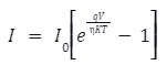
In a p-n junction diode, the current I can be expressed as
Dynamic resistance is the function of operating potential difference. It is equal to the reciprocal of the slope of i-v.
The dynamic resistance of a pn junction diode is given as
R = vi
Where,
∆v denotes the small change in the applied potential difference.
∆i denotes the corresponding small change in the current.
The extra energy is emitted in the form of a photon when a conduction electron transitions to the valence band to fill up a hole in the PN junction. The wavelength of this photon is in the visible range (380 nm-780 nm); one can see the emitted light. These kinds of PN junctions are known as light-emitting diodes.
For silicon and germanium, the wavelength of the photons falls in the infrared region.
When a potential difference is applied across a PN junction, that device conducts electricity more quickly from one terminal of the applied potential difference than from the other. Thus, a PN junction can serve as a function of a junction rectifier.
A photon is generated when an electron moves from the conduction band to the valence band. This photon stimulates a second electron to enter the valence band, producing a second photon by stimulated emission. A chain reaction of emission occurs, and a current is generated in the circuit. This leads to the generation of laser light. To bring this, the surfaces of the PN junction need to be flat and parallel to reflect the light back and forth within the crystal. Thus, a PN junction can act as a junction laser.
A PN junction is a single semiconductor crystal with one end doped to form p-type material and the other end to form n-type material. The junction plane is the meeting point of these two types.
Zener diodes, junction rectifier, junction laser and a light-emitting diode are examples of the forward current equation of the PN junction diode.
Forward pn Junction diode has numerous importance; it is used in temperature sensors, reference voltages, solar cells and digital cameras.



 Profile
 Settings
 Refer your friends
 Sign out